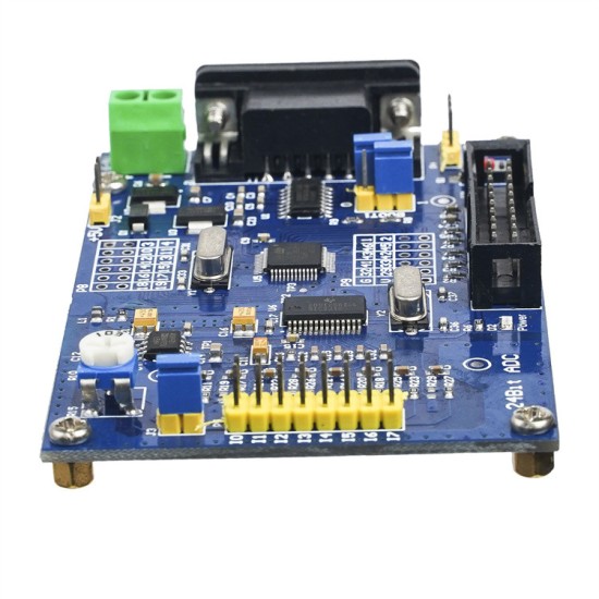


ADS1256 24 -bit AD high -precision collection module 24 -bit ADC STM32F103C8T6 AD module
Link: https://pan.baidu.com/s/1djyf- PL_MB_0rltlbupqwa extract code: 1234
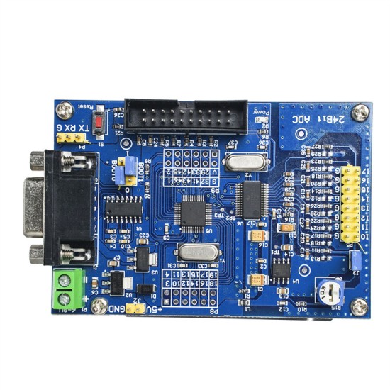
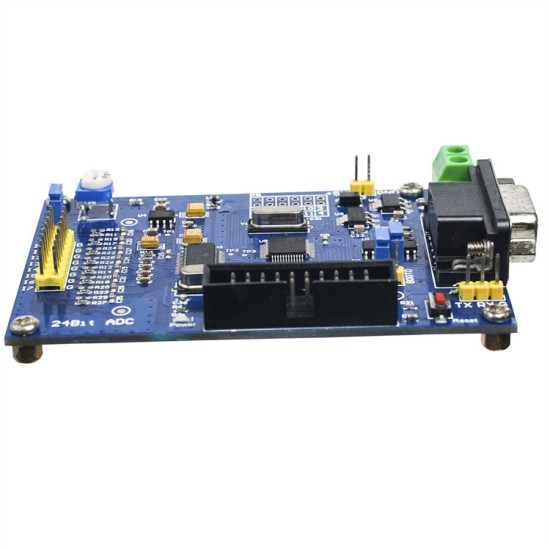
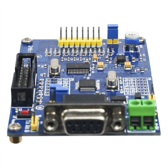
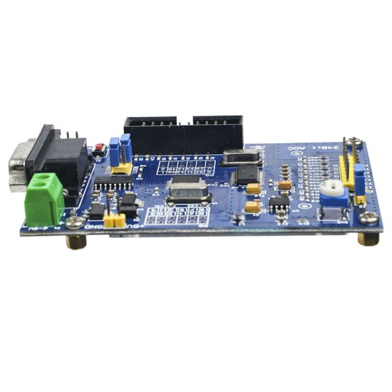
4. The new original main control MCU: STM32F103C8T6;
13. STM32F103C8T6 reset button;
5. 2.5V benchmark, super high precision, low temperature drift;
14. USB to TTL wiring, corresponding to MCU TX, RX, GND, can communicate directly with the computer;
6. Putable potentiometer, output adjustable voltage link to Ain0/ i0;
15. Original imported 3232 serial communication chip;
7. Collect 8 channels and input, i0-I7 connected to the positive end of the voltage, G is an analog ground, the connection of the collection voltage negative end;
16. String oral, mother;
8. Enter the filtering and attenuation resistance, do not do attenuation by default, leave the position of welding attenuation resistance, 0603 packaging;
17. The output voltage of the adjustable potentiometer to I0 / AIN0: disconnect the IO suspended, connect the I0 measuring potentiometer output voltage end;
9. ADS1256idb collect chip, new original import;
18. Boot0 and boot1 of STM32 select control jump cap;
Display on ground measurement results: Note that the unit is UV
As shown in the figure below: Collect the card on the card. The seven DI use the channel i7 and the simulation ground (G) to use a jump cap with a jumper to measure the simulation floor.The size of the measurement result directly reflects the layout of the layout of the board, the filter is good or bad, the smaller the sample result, the better the fluctuation, the smaller the better.For multiple model tests, the sampling voltage is in several UVs.Many other board sampling voltage on the market have hundreds of UVs. This sampling voltage will directly couple into the sampling result of the subsequent sampling, causing accuracy loss.8 channel (24bit) A/DC conversion board hardware TE:
This board has led all the IO ports of the STM32F103C8T6 single -chip microcomputer, and users can develop their own functions in the secondary development.
You can download the program through the serial port, see the description file for the specific method.Because the program can be downloaded through the serial port, there is no jlink download debugging interface on the board.
The reference voltage of AD chip is 2.5V, which is generated by precision regulatory devices.
A potentiometer is provided on the board to test the AD input. The voltage generated by the division of the potentiometer is connected to an0 by the S3 jump line, which is suitable for dying the board without a sensor.If this test is not required, you can take the S3 jump line and enter the test voltage directly from the AN0 --n7.(The voltage input to the AD input end cannot be higher than 5V)
The specific functions of the 3 modes are introduced one by one:
// Mode 1:
Continuously collect the single -channel AN0 analog voltage for ADC conversion, and calculate the conversion data as a voltage value. In the form of ASCII code, send out the data through the serial port. In this mode, the serial assistant software can directly read the voltage, suitable for software developmentEngineers are used because there is no need to understand any principle of single -chip microcomputer hardware.
The collection data shows that the following example is the result of the voltage from the DI0 channel (AN0). The measurement accuracy is very stable in the data within the range of 0.0001V (that is, 0.1MV). The rest of the channel is vacant.
Because the ASCII code is transmitted, the upper -seat serial port software should select "Display". Do not select the hexadecimal display, otherwise the garbled is displayed.
// Mode 2:
Continuously collect the 8 -channel analog voltage for 24 -bit ADC conversion, and calculate the conversion data as a voltage value. In the form of ASCII code, the data is sent through the serial port. In this modeSoftware development engineers are used because there is no need to understand any principle of single -chip machine hardware.
The collection data shows the following example:
// Mode 3:
Full differential input mode, the measured voltage range is -5V ~+5V. A total of 4 sets of differential inputs. It is suitable for sensors that connect electronic scale.
The corresponding input pin is:
An0 -------- channel 0 (V0) +input
An1 -------- channel 0 (v0) -Enter
An2 -------- channel 1 (v1) +input
An3 -------- channel 1 (v1) -Enter
An4 -------- channel 2 (v2) +input
An5 -------- channel 2 (v2) -Enter
An6 -------- channel 3 (v3) +input
An7 ------------------- Entry 1. Input 1. The power input terminal, the upper end is the ground line, and the lower end is+5V.2.LT3461 power chip, high -grained wave noise suppression ratio.
3. Power indicator light.
4.lP2985, LDO can effectively filter low -frequency noise, produce a very pure+5V, and provide analog power supply for ASD1256.
5.ADR431BRZ, B series is a high -precision benchmark.The benchmark chip, generate a high -precision 2.500000V benchmark
6. The benchmark test hole.
7. The simulation input end, AIN0-AIN7 has a total of eight input ports, can be used as 8 independent single-end inputs, and can be used for 4 sets of differential inputs. AIN0 and AIN1 are in a group. AIN2 and AIN3 AIN4 and AIN5 AIN6 and AIN7Then, then
8. Sims input port
9. Input resistance and attenuation resistance.The attenuation resistance is not welded by default.
10.Ads1256 main control chip.
11.AMS1117-3.3V, provide digital voltage for ADS1256.
12. NSK brand crystal, 7.68MHz
13. communication interface with MCU.
| Product Attributes | |
| Brand | none |
| Interface | Power module |
Unlimited Blocks, Tabs or Accordions with any HTML content can be assigned to any individual product or to certain groups of products, like entire categories, brands, products with specific options, attributes, price range, etc. You can indicate any criteria via the advanced product assignment mechanism and only those products matching your criteria will display the modules.
Also, any module can be selectively activated per device (desktop/tablet/phone), customer login status and other criteria. Imagine the possibilities.
$19.19
Price in reward points: 19
- Stock: In Stock
- Model: ULSJ1215
- Weight: 0.10kg
Available Options
This product has a minimum quantity of 10


